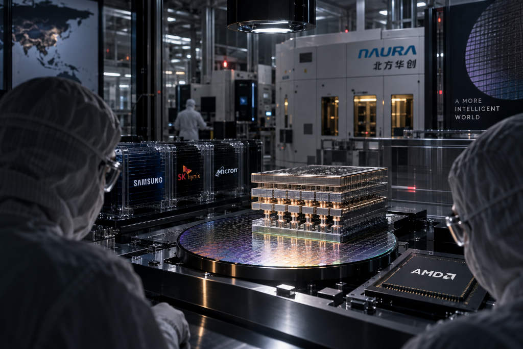
3D DRAM race heats up as AMD, NAURA and memory giants push new architectures and process tools
Two developments in the first week of September 2026 put 3D DRAM back at the center of the memory industry. AMD disclosed internal test results for a Hybrid Bonding-based 3D DRAM architecture, saying energy efficiency could improve by as much as 17x versus conventional HBM stacks. Around the same time, Chinese semiconductor equipment maker NAURA published an IEEE paper describing a manufacturing advance for next-generation 3D DRAM, including a two-step cyclic etch process for 64-layer alternating silicon and silicon-germanium structures, structural uniformity above 95%, an etch selectivity above 500:1, and silicon loss below 10 angstroms in a 200 nm interlayer structure. The report argues that these announcements matter because conventional DRAM scaling is nearing physical and economic limits. It also reviews the two main technical paths now being pursued, 4F2 VCT and VS-CAT, and outlines how Samsung Electronics, SK hynix, and Micron are positioning themselves. Beyond chipmakers, the shift is also reshaping the equipment chain, from high-aspect-ratio etch to atomic layer deposition, wafer bonding, CMP, cleaning, inspection, coating and developing, testing, and high-purity process systems.